Intel Claims Sole 300mm InP Photonics Supply [2026]

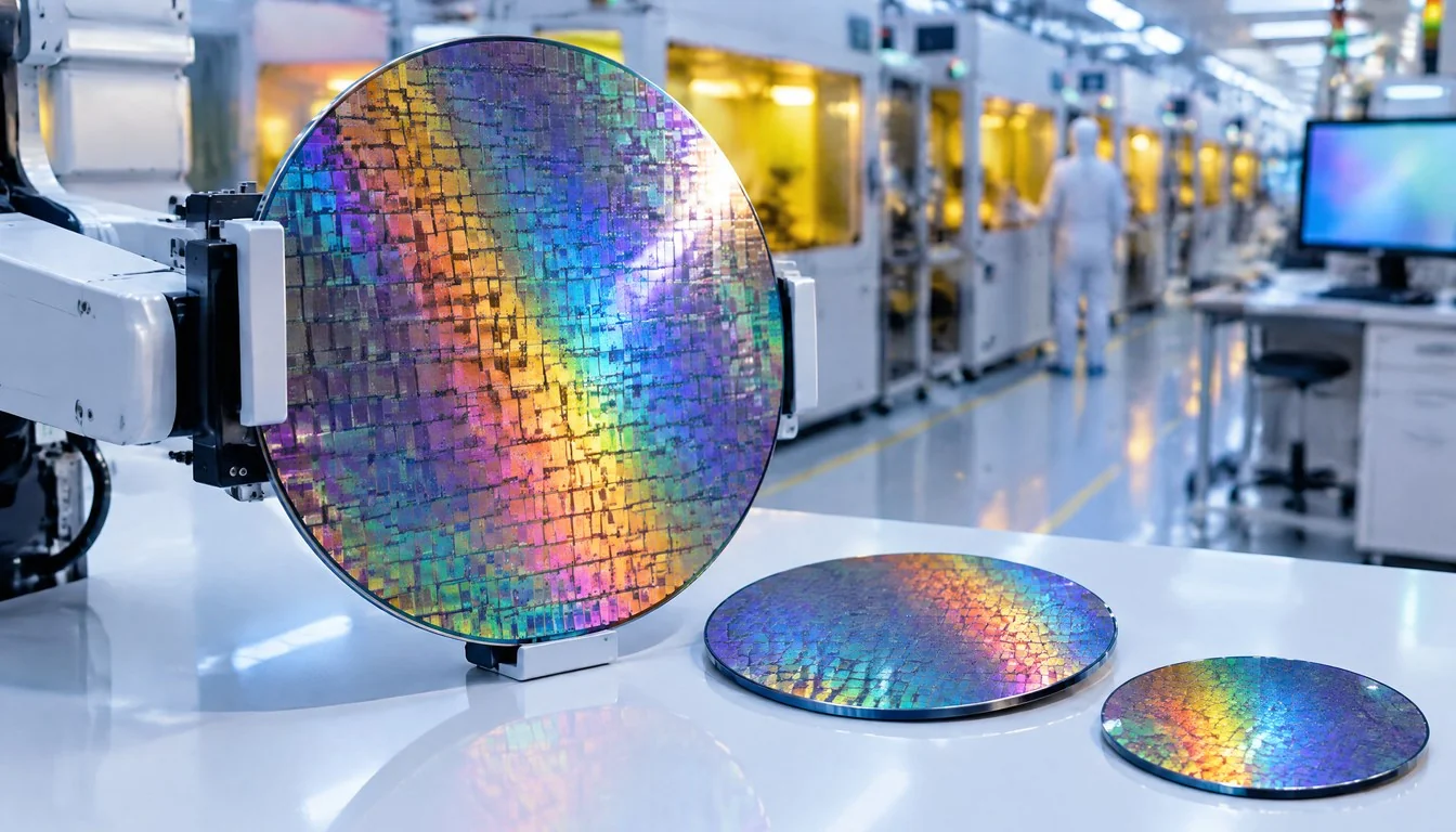
Intel says it has pulled off something no other wafer foundry can currently match: high-volume production of 300mm indium phosphide (InP) silicon photonics wafers, aimed squarely at the optical interconnects that AI data centers are going to need by the truckload. The claim surfaced at the 2026 Open Compute Project (OCP) Global Summit and was reported on October 18, 2026, by TrendForce, Wccftech, XenoSpectrum, BigGo Finance, and Compound Semiconductor. If the claim holds up under scrutiny, it hands Intel a rare manufacturing edge at the exact moment the industry is racing to solve a bandwidth and power problem that threatens to choke next-generation AI clusters.
This is not a new chip or a new GPU. It is a foundry capability claim, and the distinction matters. Intel is positioning itself as a supplier to the broader industry, not just a vendor of its own parts, which changes how customers, competitors, and investors should read the announcement. Here is what Intel actually said, what it means for co-packaged optics (CPO), and where the gaps in the public record still sit.
Don't miss new tech stories on Google
Add TrendinTech once in the Google app and our stories appear in your news suggestions.
What Intel Announced at the 2026 OCP Global Summit
At the 2026 OCP Global Summit, Intel told attendees it is currently the only high-volume wafer foundry capable of supplying 300mm InP silicon photonics to the broader industry at scale, according to TrendForce. The company framed the capability around two specific applications: near-package optics (NPO) and co-packaged optics (CPO), both aimed at artificial intelligence and high-performance computing (HPC) workloads. XenoSpectrum’s writeup of the keynote materials described the underlying process as “InP on 300mm Silicon,” a label that refers to combining indium phosphide with a 300mm-diameter silicon wafer base, not a wafer made entirely of InP crystal.
That distinction is easy to miss and important to get right. A full 300mm InP wafer would be enormously expensive and difficult to produce at scale, since InP crystal boules are naturally smaller and costlier than silicon. By integrating InP photonic elements onto a 300mm silicon base, Intel says it can apply standard high-volume silicon wafer fabrication economics to a photonics process that has historically been stuck on smaller, more expensive InP-native wafers, typically 100mm or 150mm in diameter across the industry.
The OCP Global Summit has become one of the industry’s main venues for this kind of infrastructure disclosure. It is also where Credo recently introduced its SRMO optics standard alongside seven partners, highlighting just how much of the current AI infrastructure conversation now revolves around optical interconnects rather than pure silicon compute.
What 300mm InP Silicon Photonics Actually Is
Silicon photonics uses light, rather than electrical signals, to move data between chips, boards, and racks. Indium phosphide is the material of choice for generating that light because it can efficiently produce and amplify laser signals in ways that pure silicon cannot. The challenge the industry has wrestled with for years is that InP components have traditionally been built on their own small, expensive wafers, separate from the silicon wafers used for the rest of the electronics.
Intel’s pitch is that it has found a way to integrate InP-based laser sources directly into a 300mm silicon wafer process, the same wafer diameter used across most of the modern semiconductor industry for logic and memory. Reports described this 300mm diameter as equivalent to the familiar 12-inch wafer standard. Moving photonics onto that standard wafer size, at least in theory, lets a foundry apply the same volume manufacturing techniques, equipment, and yield practices used for conventional chips to the optical components that AI systems increasingly depend on.
Why the Wafer Size Is the Real Story
The headline number here, 300mm, is doing most of the work in this story. Smaller InP wafers mean fewer usable dies per wafer, higher per-unit costs, and tighter supply. A 300mm process, by contrast, can carry dramatically more photonic devices per wafer run. That is the foundation of Intel’s claim to be the only foundry doing this at “high volume”: it is not just that the company can make InP-on-silicon devices, it is claiming it can make them at a scale that smaller InP-native wafer runs cannot match.
Co-Packaged Optics: The Problem This Is Meant to Solve
Co-packaged optics refers to placing optical transceivers directly next to, or even inside, the same package as a switch or accelerator chip, rather than routing signals through separate pluggable optical modules mounted at the edge of a rack. The goal is to cut the distance electrical signals have to travel before being converted to light, which reduces both power draw and signal loss. Near-package optics is a related but slightly less tightly integrated approach, placing the optical engine close to the compute die on the same substrate or board rather than fused into a single package.
Both approaches exist because AI training and inference clusters now move staggering volumes of data between GPUs, accelerators, and switches. Traditional pluggable optics and copper interconnects are increasingly seen as a bottleneck, both in raw bandwidth and in the electrical power consumed just moving bits around before any useful computation happens. That bottleneck is part of the same pressure driving memory makers to rethink bandwidth strategy, as seen in Micron’s HBM4 roadmap, which describes a 2.6-times increase in AI inference throughput for every 2-times increase in memory bandwidth. Optics and memory bandwidth are, in effect, two sides of the same AI infrastructure scaling problem.
Near-Package Optics vs Co-Packaged Optics
Industry discussion at the OCP Global Summit treated NPO and CPO as a progression rather than two competing standards. NPO is generally viewed as an intermediate step, keeping the optical engine physically separate but close, while CPO represents the tighter, longer-term integration goal. Intel’s announcement positioned its 300mm InP capability as a manufacturing foundation that could serve both approaches, rather than committing to one packaging architecture over the other.
Nic Dubé’s “Golden Hammer” Comment, Explained
Nic Dubé, identified in reporting as Intel’s vice president of Data Center Systems and Solutions, described silicon photonics as the “Golden Hammer” for next-generation systems, according to coverage of the OCP keynote from The Buildout and a separate report from EET-China. The phrase, as reported, frames photonics not as one component among many but as the tool Intel expects to reach for repeatedly across future system designs, from AI accelerators to networking fabric.
Framing a packaging and interconnect technology as a universal tool rather than a point solution is a notable rhetorical choice. It suggests Intel sees 300mm InP photonics less as a single product line and more as infrastructure it intends to apply broadly across its data center roadmap, assuming the manufacturing claim survives independent verification over the coming months.
The AI Data Center Bandwidth Problem Behind the Announcement
None of this is happening in a vacuum. AI training clusters built around tens of thousands of accelerators need interconnect fabric that can move enormous amounts of data between chips without burning an unreasonable share of the cluster’s total power budget on networking alone. Industry momentum behind standards work has been building for months, including the effort from Nvidia, AMD, Google, and Meta to set a shared data center grid response standard, a sign that optics and power delivery are now being treated as linked infrastructure challenges rather than separate engineering tracks.
Reports around Intel’s announcement also referenced a long-term target of under 5 picojoules per bit for future optical links, though this figure was attributed as an aspirational target rather than a demonstrated, measured result from current production. Readers should treat that number as a goal Intel and the broader photonics industry are working toward, not a verified specification of what is shipping today.
How Intel’s Claim Stacks Up Against the Rest of the Photonics Industry
Intel is not the only company chasing optical interconnects for AI infrastructure, but its claim is specifically about high-volume 300mm foundry capacity, which is a different kind of claim than most of its rivals are making. Most other players in this space are focused on module design, packaging integration, or interconnect standards rather than owning the underlying wafer-scale manufacturing process for the photonic materials themselves.
| Company or Group | Primary Focus Area | Relationship to Intel’s Claim |
|---|---|---|
| Intel | 300mm InP-on-silicon wafer manufacturing for NPO and CPO | Claims sole high-volume foundry capability at this wafer size |
| Credo | SRMO optics standard for AI interconnects, launched with seven partners | Standards and module layer, not wafer-scale InP manufacturing |
| Nvidia, AMD, Google, Meta | Data center infrastructure standards, including power and grid response | Potential customers and ecosystem partners for CPO-ready systems |
| TSMC and Samsung foundry ecosystem | Advanced logic and packaging processes, including HBM base die work | Adjacent foundry capacity; not confirmed as a 300mm InP photonics competitor |
| Broader OCP member base | Open hardware specifications for AI and cloud data centers | Audience and venue for Intel’s announcement, not a direct rival claim |
It is worth being precise about what this table does and does not show. Intel’s claim is specifically about owning high-volume 300mm InP wafer manufacturing capacity that it can sell into the broader industry. None of the other names above have made a directly competing public claim to that specific capability as of this reporting. The comparison is about where each player sits in the optics and AI infrastructure stack, not a head-to-head benchmark.
Intel’s Long and Uneven History With Silicon Photonics
Intel has been working on silicon photonics for roughly two decades, going back to early optical transceiver research programs well before CPO became an industry buzzword. The company shipped its first commercial silicon photonics optical transceivers for data centers years ago, long before AI clusters created today’s pressure for co-packaged designs. What has changed is the urgency: optical interconnects used to be a niche concern for hyperscale networking teams, and they are now a mainstream topic at an event like the OCP Global Summit because AI cluster scale has made electrical interconnects a hard physical limit.
Intel’s broader 2026 has been a mix of ambition and scrutiny across its data center and hardware businesses. The company has also been active on the regulatory side this year, including an October FCC filing challenging restrictions on certain robotics hardware, and it has repeatedly been named alongside Nvidia and Micron as a stock analysts are watching heading into quarterly earnings season. That pattern, a company making bold technical claims while also fighting on regulatory and financial fronts, is consistent with a business trying to reassert itself as a essential infrastructure supplier rather than just a CPU maker.
What’s Confirmed and What Still Needs Independent Verification
It is worth separating what multiple outlets have reported from what remains an open question. Confirmed by multiple reports: Intel made the claim at the 2026 OCP Global Summit, the claim centers on 300mm InP-on-silicon wafers, the stated applications are NPO and CPO for AI and HPC, and Nic Dubé delivered the “Golden Hammer” framing as Intel’s vice president of Data Center Systems and Solutions.
Not yet confirmed by public reporting: any specific product name built on this process, any named customer or design win, actual shipment volumes, a firm production or availability date, and pricing. The often-cited target of under 5 picojoules per bit is also described as a long-term goal rather than a measured result from current production runs. Readers and investors should treat Intel’s statement as a manufacturing capability and strategy announcement, not confirmation that commercial mass production of customer-ready CPO systems built on this process is already underway.
Market Impact: Why This Matters Beyond Intel
If Intel’s capability claim holds up, the company would have a genuine foundry-services angle into the AI infrastructure boom that does not depend on competing head-on with Nvidia’s GPUs or AMD’s accelerators. Supplying photonics wafers to the broader industry, rather than only building photonics into Intel’s own products, would make Intel a picks-and-shovels supplier for whichever GPU or accelerator ultimately wins the AI compute race. That positioning helps explain why Intel keeps surfacing in analyst notes alongside Nvidia and Micron as a stock worth watching ahead of earnings season this quarter.
It also has implications for the broader semiconductor supply chain. Memory and logic manufacturing has already been shifting toward tighter integration between packaging and compute, visible in moves like Samsung tapping TSMC’s 3nm lines for Nvidia’s next generation HBM base die. A credible high-volume InP-on-silicon process from Intel would add another layer to that same trend: foundries competing not just on transistor density, but on how well they can integrate fundamentally different materials and functions, logic, memory, and now photonics, onto standard wafer formats.
The OCP Global Summit’s Growing Weight in AI Infrastructure
The Open Compute Project started as a hyperscaler-driven effort to open-source data center hardware designs, reducing costs by standardizing server, rack, and power specifications across the industry. In 2026, the OCP Global Summit has become something closer to a venue where the industry’s biggest infrastructure bets get announced in public, from optics standards to power delivery agreements. Intel choosing this stage, rather than its own dedicated event, to make a foundry capability claim says something about where it believes the real audience sits: hyperscale buyers and systems integrators, not just end consumers or even traditional chip customers.
| Detail | What Was Reported |
|---|---|
| Company | Intel |
| Event | 2026 Open Compute Project (OCP) Global Summit |
| Date of reporting | October 18 to 20, 2026 |
| Core claim | Only high-volume foundry supplying 300mm InP silicon photonics industry-wide |
| Wafer size | 300mm (12-inch) |
| Target applications | Near-package optics (NPO) and co-packaged optics (CPO) |
| End markets cited | Artificial intelligence (AI) and high-performance computing (HPC) |
| Named executive | Nic Dubé, VP of Data Center Systems and Solutions |
| Notable quote framing | Called silicon photonics the “Golden Hammer” for next-generation systems |
| Confirmed mass production of customer systems | Not confirmed; announcement describes manufacturing capability |
What This Means for Nvidia, Broadcom, and the Optics Supply Chain
Every major AI accelerator vendor has a stake in how fast co-packaged optics matures, because every one of them eventually hits the same networking bottleneck once clusters scale past a certain size. A credible third-party InP-on-silicon supply source, separate from any single GPU vendor’s internal roadmap, would give switch and accelerator makers an additional path to source photonics components without being tied to a single vertically integrated supplier. That kind of optionality tends to matter a lot to hyperscalers that have spent the last several years trying to avoid single-source dependency on any one piece of their AI infrastructure stack, whether that is GPUs, HBM memory, or now optical interconnects.
It is also a reminder that the AI infrastructure race is no longer just about who has the fastest accelerator. Power delivery, memory bandwidth, and now optical interconnect manufacturing capacity have all become competitive battlegrounds in their own right, each with its own supply chain, standards bodies, and now, apparently, foundry capability claims that need independent verification before they reshape anyone’s product roadmap.
Predictions: Where 300mm InP Photonics Goes From Here
- Expect independent analysts and industry publications to press Intel for named customers or design wins tied to this 300mm InP process within the next two to three quarters, since capability claims without named adopters tend to draw scrutiny at the next major industry event.
- Watch for competing foundries, potentially including TSMC’s ecosystem partners, to respond with their own photonics wafer-scale announcements, given how quickly rival capability claims tend to surface once one major player stakes out ground at a venue like OCP.
- The under 5 picojoules per bit target is likely to become a benchmark the rest of the industry gets measured against in future announcements, even though it remains unverified as a shipped result today.
- Co-packaged optics adoption will likely remain concentrated in the largest hyperscaler clusters first, with broader enterprise data center adoption lagging by several years, consistent with how most AI infrastructure innovations have rolled out since the current AI buildout accelerated.
- Intel’s positioning as a foundry supplier to the broader industry, rather than solely a vertically integrated product company, is likely to keep showing up in analyst commentary alongside its CPU and GPU roadmap discussions through the rest of 2026 and into 2027.
The Bottom Line on Intel’s Photonics Claim
Intel has made a specific, bold claim: it is the only high-volume foundry able to supply 300mm InP silicon photonics to the industry at large, aimed at the co-packaged and near-package optics that AI data centers increasingly need. The claim arrived at exactly the venue where hyperscalers and systems builders gather to compare infrastructure notes, which suggests Intel wants this read as a supply chain pitch, not just a research milestone. What happens next depends on whether named customers, measured performance data, and firm production timelines follow in the coming months, or whether this settles into another chapter in Intel’s long, often frustrating history of photonics research that took years to turn into shipped volume.
Frequently Asked Questions
What did Intel announce about silicon photonics in October 2026?
Intel said it is the only high-volume wafer foundry currently able to supply 300mm indium phosphide (InP) silicon photonics to the broader industry at scale, intended for near-package optics (NPO) and co-packaged optics (CPO) in AI and HPC systems. The claim was reported on October 18, 2026, tied to the 2026 OCP Global Summit.
What is 300mm InP silicon photonics?
It refers to integrating indium phosphide, a material used to generate and amplify laser light, onto a standard 300mm (12-inch) silicon wafer base. This differs from a wafer made entirely of InP crystal, which is smaller, more expensive, and harder to produce at volume.
What is co-packaged optics, and why does it matter for AI?
Co-packaged optics places optical transceivers directly next to or inside the same package as a switch or accelerator chip, cutting the electrical distance signals travel before converting to light. This reduces power consumption and signal loss, both of which become critical as AI clusters scale to tens of thousands of interconnected accelerators.
Who is Nic Dubé and what did he say?
Nic Dubé is identified in reports as Intel’s vice president of Data Center Systems and Solutions. He described silicon photonics as the “Golden Hammer” for next-generation systems during Intel’s presentation at the OCP Global Summit.
Has Intel actually started mass production of these wafers?
Intel’s statement describes a high-volume manufacturing capability, but public reporting has not confirmed that commercial mass production for named customer products is already underway. Specific product models, customers, shipment volumes, and firm availability dates remain unconfirmed as of this reporting.
How does Intel’s claim compare to Nvidia, Broadcom, or Credo in photonics?
Intel’s claim is specifically about owning high-volume 300mm InP wafer-scale manufacturing, a foundry-level capability. Other players in this space, including Credo with its recently launched SRMO optics standard, are generally focused on module design, packaging, or interconnect standards rather than owning this specific wafer manufacturing process.
What is the OCP Global Summit?
The Open Compute Project Global Summit is an annual event where hyperscalers, chipmakers, and systems builders present open hardware specifications and infrastructure announcements for cloud and AI data centers. It has become a major venue for optics, power delivery, and interconnect announcements tied to AI infrastructure scaling.
What is still unverified about Intel’s 300mm InP photonics claim?
The reported long-term target of under 5.5 picojoules per bit is described as an aspirational goal rather than a measured, shipped result. No specific product model, named customer, shipment volume, production date, or price has been confirmed in public reporting as of October 20, 2026.
Related Coverage
Owen Castellanos
Owen Castellanos is the Hardware & Gaming Reporter at TrendinTech, where he tests graphics cards, processors, consoles and peripherals and follows the games industry, from the major publishers to independent studios. He writes for readers who want to know whether a product is worth the money, and he is not shy about saying when it is not.
All stories by Owen Castellanos (403)