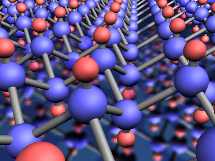
A collaboration of engineers and scientists led by UCLA has developed a method for creating a new kind of superlattice that use alternating layers of two-dimensional sheets that are only a few atoms thick at the most.
These new superlattices are unlike anything scientists have ever created previously. One layer of the new kind of superlattice allows free-flowing electrons to swiftly pass through while the other layers act as an insulator. Being designed in this way ensures that the electronic and optical properties are confined to single layers, meaning they’re less likely to interfere with other layers.
Superlattices such as these can be the basis for a whole new class of electronic and optoelectronic devices. Such applications would include things like advanced LEDs and lasers and superfast semiconductors for transistors in various smart technologies.
This new method developed to create 2D superlattices is much more efficient than the conventional methods in place today. The way in which these superlattices are created uses alternating 2D atomic crystal sheets that are interspaced with molecules of different shapes and sizes. This layer is held in place by weak electrostatic forces known as “van der Waals” forces acting as a second sheet. These new superlattices are now referred to as “monolayer atomic crystal molecular superlattices.”
“Traditional semiconductor superlattices can usually only be made from materials with high similar lattice symmetry, normally with rather similar electronic structures,” said co-author of the study and UCLA professor of materials science and engineering at the UCLA Samueli School of Engineering, Yu Huang. “For the first time, we have created stable superlattice structures with radically different layers, yet nearly perfect atomic-molecular arrangements within each layer.”
One method that’s currently used to build superlattices involves stacking the ultrathin layers on top of one another. The problem with this method is that it’s very labor intensive. And, due to the fragile parts involved it takes a long time to build. Another method involves growing a new layer on top of the existing one via a process called “chemical vapor deposition.” However, that method is also very labor intensive and has low yield rates.
The new method involves applying a negative voltage to the 2D material through a process called “electrochemical intercalation.” As the negatively charged ions are injected into the material, it attracts positively charged ammonium molecules to the area situated between the atomic layers. These molecules then assemble into new layers automatically, creating what’s now known as a superlattice.
“Think of a two-dimensional material as a stack of playing cards, said Xiangfeng Duan, a lead of the study and UCLA professor of chemistry and biochemistry. “Then imagine that we can cause a large pile of nearby plastic beads to insert themselves, in perfect order, sandwiching between each card. That’s the analogous idea, but with a crystal of 2D material and ammonium molecules.”
To begin with, the team used black phosphorus to act as a base 2D atomic crystal material. After their success with that, they moved on to try different types of ammonium molecules of varying size and symmetry to create a whole range of nee superlattices. What the researchers discovered was that they could customize the structures of the layers of these new superlattices, meaning they could be great for making much faster transistors that are far more efficient than any that we have in use today.

