Researchers at MIT have been working with various materials looking for ways to improve their electrical conductivity. Working with one particular clear, conductive coating, they may have just solved the issue – one which could potentially increase the efficiency (and stability) of solar cells and touch screen technology tenfold.
The material most commonly used in things such as solar cells and touch screens is indium titanium oxide – otherwise known as ITO. And while it does do the job of acting as a good conductor of electricity, its structure is quite brittle and easy to crack. While one of the same researchers on this project, Professor Karen Gleason, and colleagues, did improve a version of this material a couple of years ago, it was nowhere near as conductive or transparent as ITO. The new structured material, however, is much better.
Siemens per centimeter is the measurement unit used when calculating the combined transparency and conductivity of a material. ITO ranges from between 6000 to around 10000 Siemens per centimeter, which is pretty incredible. In this new research, the aim was to find a material that could reach a minimum of 35 – it reached a staggering 3000. And even still, there’s room for improvement, say the team.
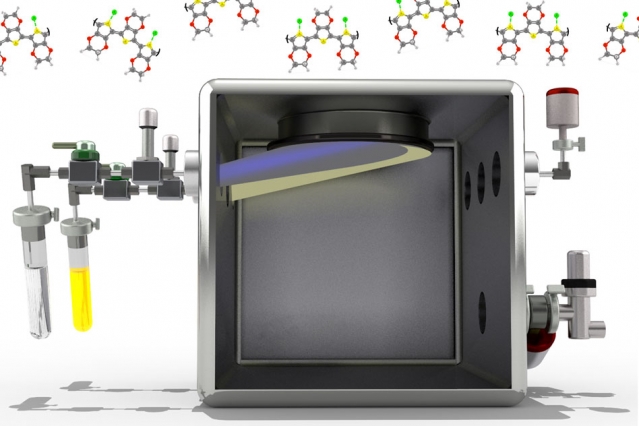
The new, flexible material is called PEDOT. It’s an organic polymer that’s spread out in an ultra-thin layer via a process known as oxidative chemical vapor deposition (oCVD). This is what gives the material such as high conductivity. To demonstrate this, the team applied a layer of PEDOT into a solar cell. The new combination proved to be very complementary. Not only did the efficiency of the solar cell improve, but its stability doubled also.

Illustration courtesy of the authors, edited by MIT News
While these initial tests involved substrates just 6 inches in diameter, the team is confident it can be applied on a much larger scale during manufacturing processes. Creating the oCVD and applying it to substrates is a relatively easy process that’s ideal for use on things such as flexible solar cells and screens. It’s a breathable material that can coat even the finest contours of an object.
The team will still need to demonstrate the material’s efficiency on a larger scale and show it’s efficiency levels over time, but overall, it’s a very good result indeed.
