For quite some time now, graphene has been one of the most versatile materials known to man. It’s used in solar cells, drug delivery, and biosensors among other things. And now, thanks to a group of engineers at the UCLA Samueli School of Engineering it’s been used to develop a new kind of photodetector that could vastly improve thermal sensing, night vision, and medical imaging.
Photodetectors are sensors of light that are found in cameras and other imaging devices. They create images by sensing the patterns of photons. There are different photodetectors that sense different parts of the light spectrum. For example, those used in night vision goggles work by sensing thermal radion undetectable to the naked eye. Others are used to identify chemicals within the environment. These work by detecting how they reflect light.
Their operating speed, sensitivity levels to lower light, and how much of the spectrum they’re able to sense are the three things that largely decide how useful and versatile the photodetectors are. Traditionally when engineers made improvements to one of these areas at least one of the other areas would diminish as a result. But, this new photodetector developed by the UCLA engineers has significantly improved in all three areas.

“Our photodetector could extend the scope and potential uses of photodetectors in imaging and sensing systems,” says Mona Jarrahi, lead author of the study and a professor of electrical and computer engineering. “It could dramatically improve thermal imaging in night vision or in medical diagnosis applications where subtle differences in temperatures can give doctors a lot of information on their patients. It could also be used in environmental sensing technologies to more accurately identify the concentration of pollutants.”
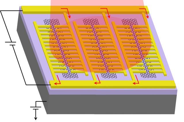
In order to develop the photodetector, the engineers first have to lay strips of graphene over a silicon diode layer which sat on a base layer of silicon. They then had to create a number of comb-like nanoscale patterns made using gold. The graphene was used as a kind of net in which to catch any incoming photons and transform them into an electrical signal. While the gold nanopatterns were used to transfer that information quickly to a processor which then produces a high-quality image as a result.
More News to Read
- UCLA Scientists Report Their Deepest Understanding Yet of the Enzyme Telomerase
- The World’s Most Sensitive Experiment for Dark Matter is Now Underway
- On the Hunt for Clandestine Nuclear Weapon Sites
- Without Teamwork, There will be No Colonizing on Mars
- Engineers Develop A New Cloaking Material That Can Hide Hot Objects

