NASA founded CMOS technology that is responsible for image sensors found on almost all devices. In dental x-ray, CMOS imagers reduce susceptibility to electrical noise while giving dentists images they can manipulate for more accurate diagnoses. Since NASA is famous for capturing all sorts of images that have significant scientific value for analysis, CMOS imagers in dental x-ray are a big deal.
NASA’s 1980s charge coupled device (CC) technology resulted in the first digital cameras. From there, the quest for faster, better, cheaper imaging has been expanded. In dental technology, CCD-based pixel arrays work in pointing accurate images. NASA engineer Eric Fossum thought amplified images might be supplanted by CMOS or complementary metal oxide semiconductor technology.
The budding active pixel technology still requires a lot of development before it can be commercialized. Thus, JPL entered several technology corporation agreements (TCA) with industry partners. Equipment expertise and resources were exchanging in working towards advancing new camera-on-a-chip technology. During this period, the CMOS sensor chip was developed. What followed was efforts of working out idiosyncrasies inherent to adapting the technology for x-ray use. That is when the companies collaborated with Photobit 1995.
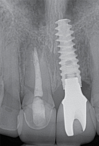
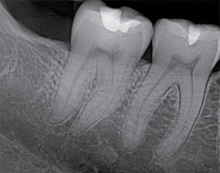
CMOS pixel arrays are more proficient, especially for battery-powered devices. That is where camera electronics come into the picture. Thus, CCD technology retained an advantage in panoramic imaging. Fast forward to modern dental implant, this technology is fundamental for every procedure.
Modern day dental images continuously benefit not only from the initially enhanced capabilities of NASA’s CMOS but also from rapid improvement, as well as reduced costs that have come as a result of active pixel sensor technology explosion. Companies such as Schick have helped JPL’s initiatives and turned experimental technology into useful tools in dental x-ray.
More News To Read


